Power Save
Overview
Application Scenario
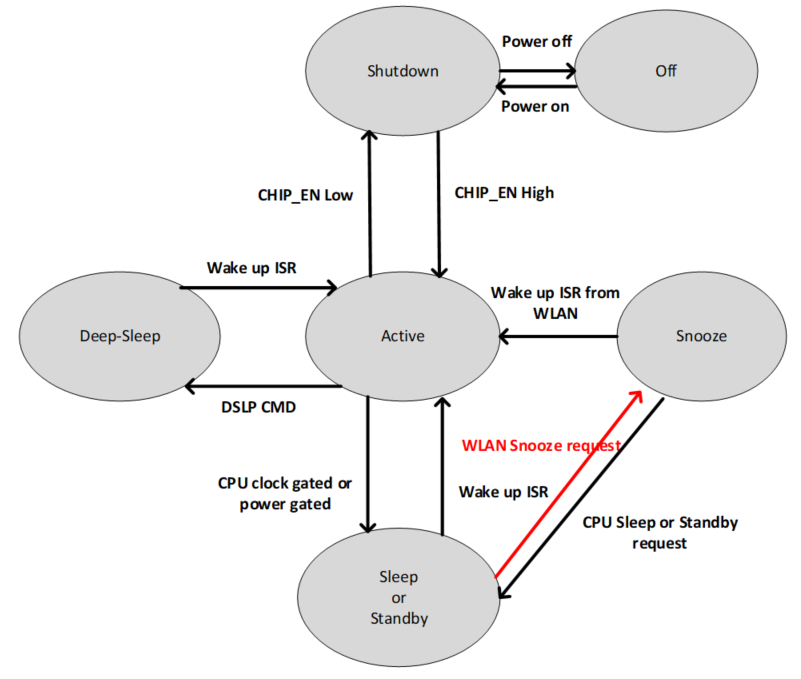
AmebaPro2 achieves low power consumption with a combination of several proprietary technologies. The power-saving architecture features six reduced power modes of operation: active, sleep, standby, snooze, deepsleep, shutdown mode. With the elaborate architecture, the battery life of whole IOT system could be extended.
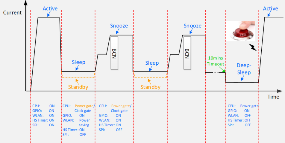
For reading pen application, it can divide into three-scenario. First, press the power button to power on reading pen to active mode and then connect to the cloud to download data. Second, once the reading pen without any activity for 2 minutes, the system will go to sleep mode (for system fast resume and keep WIFI connect) or standby mode (for lower power consumption and keep WIFI connect) and regularly wake up to receive WLAN beacon while into snooze mode. At last, without using the reading pen exceeds 10 minutes, the system will into deep sleep mode and waiting for any button signals to wake up system into active mode. The application scenario flow was shown in

Features
Active Mode: The CPU is in active mode and all peripherals are available.
Sleep Mode: The CPU is in clock-gated and can be woken up by most of peripherals. The system resume time could be much faster than the Standby mode and the WLAN could be ON or power saving mode in this state.
Standby Mode: The CPU is in power-gated and can be woken up by most of peripherals. The power consumption could be lower than the Sleep mode and the WLAN could be ON or power saving mode in this state.
Snooze Mode: In this mode system can regularly wake up to receive WLAN beacon without software intervention. The significant difference between Snooze and Sleep/Standby mode is WLAN capability and could be receive and transmit beacon in this state.
DeepSleep Mode: The lowest power consumption than the other power mode except for shutdown mode, it can be only woken up by LP Timer or GPIO.
Shutdown Mode: The CPU will be shutdown while CHIP_EN was Low.
Power Mode and Power Consumption
The mode transition diagram is given in.

In Figure, the power mode can be divided into 6 states except for “off” state and the each power In Figure, the power mode can be divided into 6 states except for “off” state and the each power consumption was shown in Figure. The introduction of each power mode, clock-gated and power-gated state will be in the following sections. Clock/power gated state could be regarded as a status of any hardware.
Deep Sleep Mode
CHIP_EN keeps high. User can invoke Deep Sleep API to force into deep sleep mode. By using specified interrupts to wake up system.
The following wake flow: Wake up ISR is high -> PMC -> enable CPU -> Reboot flow.
Wakeup Source
Aon GPIO, RTC, comparator, Aon Timer
Aon GPIO: GPIOA0~GPIOA3
Comparator: GPIOA0~GPIOA3
Standby Mode
CHIP_EN keeps high. User can invoke Standby API to force into deep sleep mode. By using specified interrupts to wake up system.
The following wake flow: Wake up ISR is high -> PMC -> enable CPU -> Fast reboot flow.
Wakeup Source
Aon GPIO, RTC, comparator, Aon Timer, Gtimer0, PWM, Pon GPIO, Uart0, Wlan
Aon GPIO: GPIOA0~GPIOA3
Pon GPIO: GPIOF0~GPIOF17
Comparator: GPIOA0~GPIOA3
Note
The clock source of gtimer0 and Uart0 only support 4MHz clk.
Sleep Mode
CHIP_EN keeps high. User can invoke Sleep API to force system into deep sleep mode. By using specified interrupts to wake up system.
The following wake flow: Wake up ISR is high -> PMC -> enable CPU -> Execution of instructions continues.
Wakeup Source
Aon GPIO, RTC, comparator, Aon Timer, Gtimer0, PWM, Pon GPIO, Uart0, Wlan
Aon GPIO: GPIOA0~GPIOA3
Pon GPIO: GPIOF0~GPIOF17
Comparator: GPIOA0~GPIOA3
Set AON GPIO pull control before power save mode
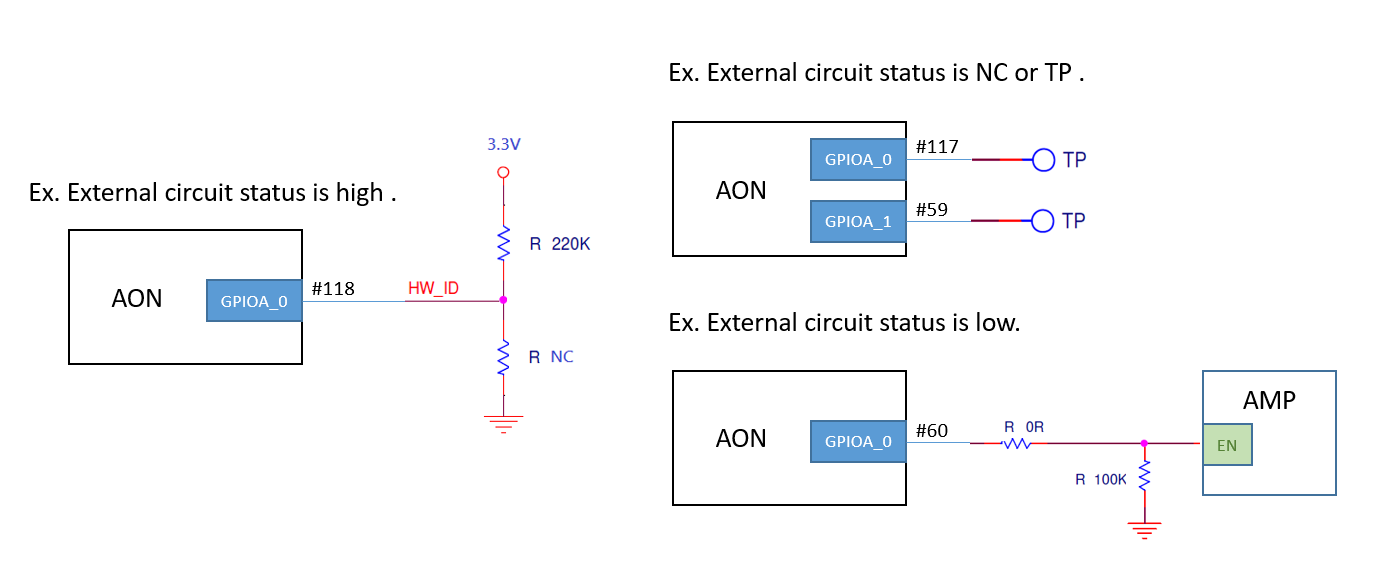
Check the AON GPIO external circuit status and set the AON GPIO states matching the external circuit to prevent leakage.
External pull high → internal pull high
External pull low or floating → internal pull low
For the detailed definition of AON GPIO control register, please refer to rtl8735b_aon_type.h.
#define AON_SHIFT_AON_GPIO1_SLEW_RATE                28
#define AON_BIT_AON_GPIO1_SLEW_RATE                  ((u32)0x00000001 << 28)    /*!<R/W 0  0:Disable,1:Enable */
#define AON_SHIFT_AON_GPIO1_DRIVING                  26
#define AON_MASK_AON_GPIO1_DRIVING                   ((u32)0x00000003 << 26)    /*!<R/W 0  0:4mA, 1:8mA */
#define AON_SHIFT_AON_GPIO1_SMT_EN                   25
#define AON_BIT_AON_GPIO1_SMT_EN                     ((u32)0x00000001 << 25)    /*!<R/W 0  Enable AON GPIO1 Schmitt trigger; 1: enable */
#define AON_SHIFT_AON_GPIO1_PULL_CTRL                22
#define AON_MASK_AON_GPIO1_PULL_CTRL                 ((u32)0x00000003 << 22)    /*!<R/W 0  2b'00: high impedence; 2b'01: pull low; 2b'10: pull high; 2b'11: reserved */
#define AON_SHIFT_AON_GPIO1_PINMUX_SEL               16
#define AON_MASK_AON_GPIO1_PINMUX_SEL                ((u32)0x0000000F << 16)    /*!<R/W 1111  0000: Comparator_ADC 0001: I2C0_SDA 0010: 0011:JTAG_CLK/SWD_CK 0100: 0101: 0110: 0111: 1000: 1001: 1010: 1011: 1100: 1101: 1110: 1111: GPIO */
#define AON_SHIFT_AON_GPIO0_SLEW_RATE                12
#define AON_BIT_AON_GPIO0_SLEW_RATE                  ((u32)0x00000001 << 12)    /*!<R/W 0  0:Disable,1:Enable */
#define AON_SHIFT_AON_GPIO0_DRIVING                  10
#define AON_MASK_AON_GPIO0_DRIVING                   ((u32)0x00000003 << 10)    /*!<R/W 0  0:4mA, 1:8mA */
#define AON_SHIFT_AON_GPIO0_SMT_EN                   9
#define AON_BIT_AON_GPIO0_SMT_EN                     ((u32)0x00000001 << 9)     /*!<R/W 0  Enable AON GPIO0 Schmitt trigger; 1: enable */
#define AON_SHIFT_AON_GPIO0_PULL_CTRL                6
#define AON_MASK_AON_GPIO0_PULL_CTRL                 ((u32)0x00000003 << 6)     /*!<R/W 0  2b'00: high impedence; 2b'01: pull low; 2b'10: pull high; 2b'11: reserved */
#define AON_SHIFT_AON_GPIO0_PINMUX_SEL               0
#define AON_MASK_AON_GPIO0_PINMUX_SEL                ((u32)0x0000000F << 0)     /*!<R/W 1111  0000: Comparator_ADC 0001: I2C0_SCL 0010: 0011: JTAG_TMS/SWD_IO 0100: 0101: 0110: 0111: 1000: 1001: 1010: 1011: 1100: 1101: 1110: 1111: GPIO */
Set PON GPIO pull control before standby
If PON GPIO is set as standby wake up source, please check the PON GPIO external circuit status first, and set the PON GPIO status matching the external circuit before standby to prevent leakage.
External pull high → internal pull high
External pull low or floating → internal pull low

For the detailed definition of PON GPIO control register, please refer to rtl8735b_pon_type.h.
#define PON_MASK_PON_GPIO1_DRIVING                   ((u32)0x00000003 << 26)      /*!<R/W 0  0:4mA, 1:8mA */
#define PON_SHIFT_PON_GPIO1_SMT_EN                   25
#define PON_BIT_PON_GPIO1_SMT_EN                     ((u32)0x00000001 << 25)      /*!<R/W 0  Enable PON GPIO1 Schmitt trigger; 1: enable */
#define PON_SHIFT_PON_GPIO1_PULL_CTRL                22
#define PON_MASK_PON_GPIO1_PULL_CTRL                 ((u32)0x00000003 << 22)      /*!<R/W 0  2b'00: high impedence; 2b'01: pull low; 2b'10: pull high; 2b'11: reserved */
#define PON_SHIFT_PON_GPIO1_PINMUX_SEL               16
#define PON_MASK_PON_GPIO1_PINMUX_SEL                ((u32)0x0000000F << 16)      /*!<R/W 1111  0000: ADC1 0001: I2C1_SCL 0010: 0011: RFE_CTRL_0 0100: 0101: 0110:UART1_CTS 0111: 1000: 1001: 1010: 1011: 1100: 1101: 1110: 1111: GPIO */
#define PON_SHIFT_PON_GPIO0_SLEW_RATE                12
#define PON_BIT_PON_GPIO0_SLEW_RATE                  ((u32)0x00000001 << 12)      /*!<R/W 0  0:Disable,1:Enable */
#define PON_SHIFT_PON_GPIO0_DRIVING                  10
#define PON_MASK_PON_GPIO0_DRIVING                   ((u32)0x00000003 << 10)      /*!<R/W 0  0:4mA, 1:8mA */
#define PON_SHIFT_PON_GPIO0_SMT_EN                   9
#define PON_BIT_PON_GPIO0_SMT_EN                     ((u32)0x00000001 << 9)       /*!<R/W 0  Enable PON GPIO0 Schmitt trigger; 1: enable */
#define PON_SHIFT_PON_GPIO0_PULL_CTRL                6
#define PON_MASK_PON_GPIO0_PULL_CTRL                 ((u32)0x00000003 << 6)       /*!<R/W 0  2b'00: high impedence; 2b'01: pull low; 2b'10: pull high; 2b'11: reserved */
#define PON_SHIFT_PON_GPIO0_PINMUX_SEL               0
#define PON_MASK_PON_GPIO0_PINMUX_SEL                ((u32)0x0000000F << 0)       /*!<R/W 1111  0000: ADC0 0001: 0010: 0011: 0100: 0101: 0110: 0111: 1000: 1001: 1010: 1011: 1100: 1101: 1110: 1111: GPIO */
Default settings for EVB.
//AON_GPIO
    HAL_WRITE32(0x40009094, 0x0, 0x4f004f); //GPIOA_1/GPIOA_0
    HAL_WRITE32(0x40009098, 0x0, 0x4f004f); //GPIOA_3/GPIOA_2
    HAL_WRITE32(0x4000909c, 0x0, 0x4f004f); //GPIOA_5/GPIOA_4


//PON_GPIO
    HAL_WRITE32(0x40009850, 0x0, 0x4f004f); //GPIOF_1/GPIOF_0
    HAL_WRITE32(0x40009854, 0x0, 0x8f004f); //GPIOF_3/GPIOF_2
    HAL_WRITE32(0x40009858, 0x0, 0x4f008f); //GPIOF_5/GPIOF_4
    HAL_WRITE32(0x4000985c, 0x0, 0x4f004f); //GPIOF_7/GPIOF_6
    HAL_WRITE32(0x40009860, 0x0, 0x4f004f); //GPIOF_9/GPIOF_8
    HAL_WRITE32(0x40009864, 0x0, 0x4f004f); //GPIOF_11/GPIOF_10
    HAL_WRITE32(0x40009868, 0x0, 0x4f004f); //GPIOF_13/GPIOF_12
    HAL_WRITE32(0x4000986C, 0x0, 0x4f004f); //GPIOF_15/GPIOF_14
    HAL_WRITE32(0x40009870, 0x0, 0x4f004f); //GPIOF_17/GPIOF_16
//HAL_WRITE32(0x4000Ae04, 0x0, 0x20000); //GPIOF_17(VDD_DDR_EN) INPUT MODE
Get Wake Reason
The reason for triggering the wakeup can be obtained through Get_wake_reason(). Bit[9] ~ Bit[12] are based on the GPIO initialization sequence and do not directly correspond to GPIOA_0-4
/**
 *  @brief The function for get wake up reason.
 *  @returns wake up status
 *   wake up status:
 *                - bit[12]: the AON GPIO3 Wake up status.
 *                - bit[11]: the AON GPIO2 Wake up status.
 *                - bit[10]: the AON GPIO1 Wake up status.
 *                - bit[9]: the AON GPIO0 Wake up status.
 *                - bit[8]: the RTC Wake up status.
 *                - bit[7]: the COMP Wake up status.
 *                - bit[6]: the AON TIMER Wake up status.
 *                - bit[5]: the UART Wake up status.
 *                - bit[4]: NA.
 *                - bit[3]: the WLAN Wake up status.
 *                - bit[2]: NA.
 *                - bit[1]: the PON GPIO Wake up status.
 *                - bit[0]: the GTimer0 Wake up status.
 */
u32 Get_wake_reason(void);