Using JTAG/SWD to debug
JTAG/SWD is a universal standard for chip internal test. The external JTAG interface has four mandatory pins, TCK, TMS, TDI and TDO, and an optional reset, nTRST, JTAG-DP and SW-DP also require a separate power-on reset: nPOTRST. The external SWD interface requires two pins: bidirectional SWDIO signal and a clock, SWCLK, which can be input or output from the device.
SWD connection
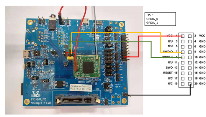
AmebaPro2 supports J-Link debugger. We need to connect the SWD connector to J-Link debugger. The SWD connection is shown as below. After finished these configurations, please connect it to PC side. Note that if you are using Virtual Machine as your platform, please make sure the USB connection setting between VM host and client is correct so that the VM client can detect the device.

Note
EVB 1V0 module needs to HW rework, ask FAE for details
Note
To be able to debugger AmebaPro2 which is powered by Cortex-M33, user needs a J-Link debugger with the latest hardware version (Check https://wiki.segger.com/Software_and_Hardware_Features_Overview for details). J-Link EDU with hardware version V10 is used to prepare this document
Software installation
To be able to use J-Link debugger, user needs install J-Link GDB server first. For Windows, please check http://www.segger.com and download “J-Link Software and Documentation Pack” (https://www.segger.com/downloads/jlink).
Setup environment
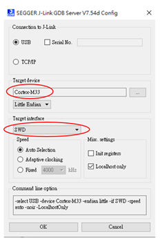
To check whether the connection works fine, user can go to the location of SEGGER J-Link tool and run “JLinkGDBServer.exe”. Choose target device Cortex-M33 (for AmebaPro2), and target interface SWD. Click “OK”

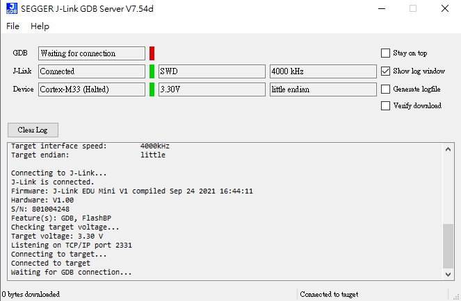
If connection succeeds, J-Link GDB server must show as below:

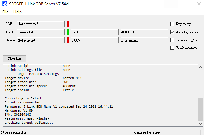
If connection fails, J-Link GDB will show:
